What is the 3D IC Packaging Market (Heterogeneous Integration) size?
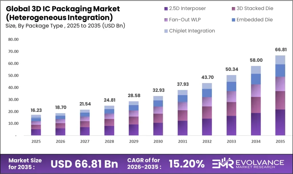
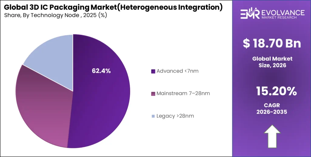
The global 3D IC packaging (heterogeneous integration) market is valued at USD 18.70 billion in 2026 and is projected to reach USD 66.81 billion by 2035, growing at a CAGR of 15.2% during the forecast period 2026 to 2035. Surging demand for heterogeneous integration architectures, escalating compute density requirements in data center AI accelerators, and the structural limits of planar Moore’s Law scaling are the primary forces driving this expansion across chiplet-based design, advanced packaging substrates, and 3D stacked memory solutions.
Semiconductor supply chain economics are reshaping the 3D IC packaging competitive landscape with unprecedented speed. Fabless design houses previously relying exclusively on leading-edge transistor scaling are committing aggressively to heterogeneous integration roadmaps — co-packaging logic, memory, analog, and RF functions at die-level rather than integrating on monolithic silicon. TSMC’s Chip-on-Wafer-on-Substrate (CoWoS) and Integrated Fan-Out (InFO) advanced packaging lines collectively grew over 35% year-over-year in 2024, with CoWoS capacity constraints becoming a binding supply bottleneck for AI GPU shipments from NVIDIA, AMD, and Broadcom. Combined capital commitments across ASE Group, Amkor Technology, TSMC, Intel Foundry, and Samsung Foundry for 3D packaging capacity expansion exceed USD 15 billion through 2028.
3D IC Packaging Market Highlights: Key Data at a Glance
- Market value: USD 18.70 billion in 2026, forecast to USD 66.81 billion by 2035 at 15.2% CAGR
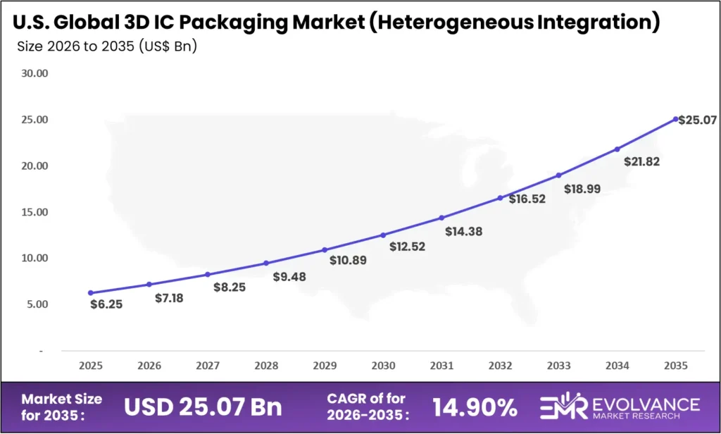
- US market: USD 7.18 billion in 2026, forecast to USD 25.07 billion by 2035 at 14.9% CAGR
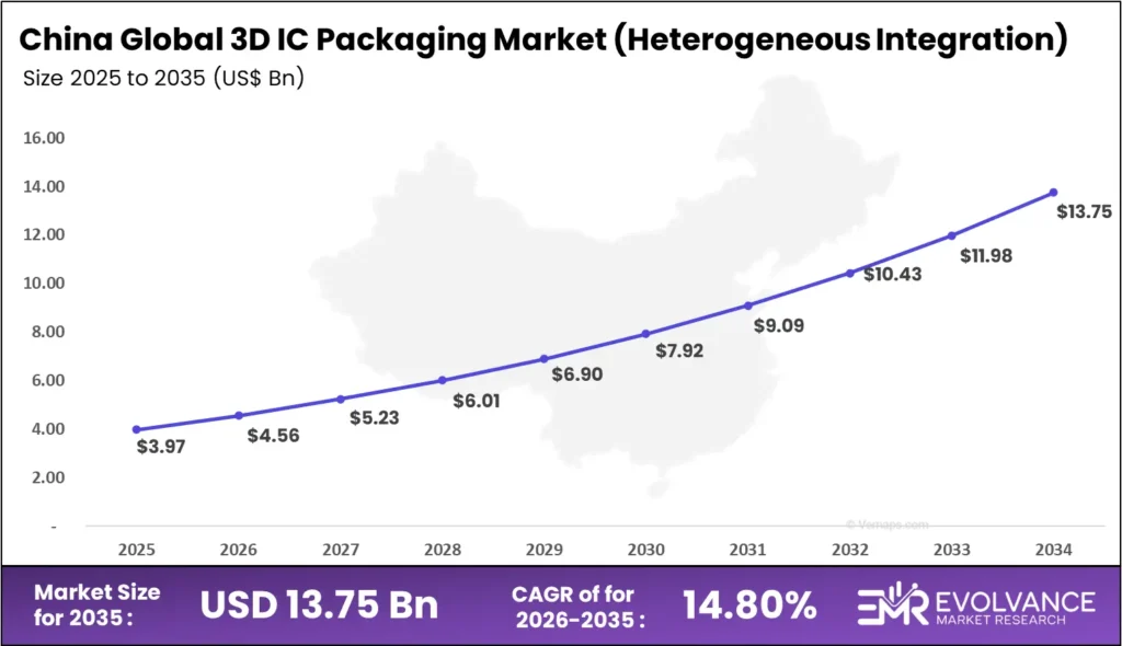
- China market: USD 4.56 billion in 2026, forecast to USD 15.78 billion by 2035 at 14.8% CAGR
- Dominant package type: 2.5D Interposer with 38.2% revenue share, driven by AI GPU and HPC co-packaging demand
- Dominant technology: Advanced Node (<7nm) with 51.6% revenue share anchoring NVIDIA H-series and AMD MI-series GPU packaging
- Dominant bonding technology: Through-Silicon Via (TSV) with 42.8% revenue share enabling high-bandwidth memory stacking
- Dominant end-use: Data Center & HPC with 39.4% revenue share, led by AI accelerator packaging demand
- Dominant application: Logic-on-Logic integration with 34.7% revenue share driven by chiplet disaggregation architectures
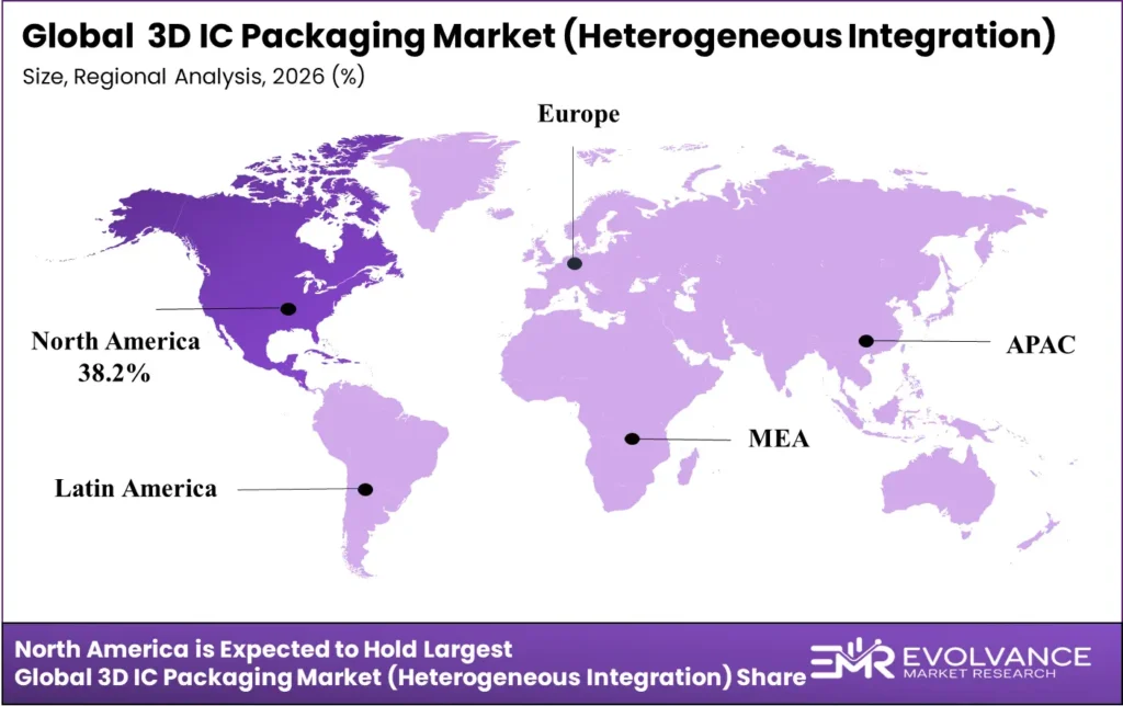
- North America: Largest regional share at 38.2%, valued at USD 8.25 billion in 2026
- Asia-Pacific: Fastest-growing region globally at 17.1% CAGR, led by Taiwan, South Korea, and China foundry expansions
What is the 3D IC Packaging Market (Heterogeneous Integration) size?
The global 3D IC packaging (heterogeneous integration) market is valued at USD 18.70 billion in 2026 and is projected to reach USD 66.81 billion by 2035, growing at a CAGR of 15.2% during the forecast period 2026 to 2035. Surging demand for heterogeneous integration architectures, escalating compute density requirements in data center AI accelerators, and the structural limits of planar Moore’s Law scaling are the primary forces driving this expansion across chiplet-based design, advanced packaging substrates, and 3D stacked memory solutions.
Semiconductor supply chain economics are reshaping the 3D IC packaging competitive landscape with unprecedented speed. Fabless design houses previously relying exclusively on leading-edge transistor scaling are committing aggressively to heterogeneous integration roadmaps — co-packaging logic, memory, analog, and RF functions at die-level rather than integrating on monolithic silicon. TSMC’s Chip-on-Wafer-on-Substrate (CoWoS) and Integrated Fan-Out (InFO) advanced packaging lines collectively grew over 35% year-over-year in 2024, with CoWoS capacity constraints becoming a binding supply bottleneck for AI GPU shipments from NVIDIA, AMD, and Broadcom. Combined capital commitments across ASE Group, Amkor Technology, TSMC, Intel Foundry, and Samsung Foundry for 3D packaging capacity expansion exceed USD 15 billion through 2028.
3D IC Packaging Market Highlights: Key Data at a Glance
- Market value: USD 18.70 billion in 2026, forecast to USD 66.81 billion by 2035 at 15.2% CAGR
- US market: USD 7.18 billion in 2026, forecast to USD 25.07 billion by 2035 at 14.9% CAGR
- China market: USD 4.56 billion in 2026, forecast to USD 15.78 billion by 2035 at 14.8% CAGR
- Dominant package type: 2.5D Interposer with 38.2% revenue share, driven by AI GPU and HPC co-packaging demand
- Dominant technology: Advanced Node (<7nm) with 51.6% revenue share anchoring NVIDIA H-series and AMD MI-series GPU packaging
- Dominant bonding technology: Through-Silicon Via (TSV) with 42.8% revenue share enabling high-bandwidth memory stacking
- Dominant end-use: Data Center & HPC with 39.4% revenue share, led by AI accelerator packaging demand
- Dominant application: Logic-on-Logic integration with 34.7% revenue share driven by chiplet disaggregation architectures
- North America: Largest regional share at 38.2%, valued at USD 8.25 billion in 2026
- Asia-Pacific: Fastest-growing region globally at 17.1% CAGR, led by Taiwan, South Korea, and China foundry expansions
US 3D IC Packaging Market
The US 3D IC packaging market will reach USD 25.07 billion by 2035 from USD 7.18 billion in 2026, growing at a CAGR of 14.9%. The United States commands the largest absolute revenue position, anchored by hyperscaler AI infrastructure investment from Microsoft Azure, AWS, Google Cloud, and Meta AI — all primary demand nodes for NVIDIA, AMD, and Broadcom AI accelerators requiring CoWoS and other 3D packaging solutions. Intel’s domestic advanced packaging strategy, reinforced by CHIPS Act funding, is adding US-based assembly and test capacity for the first time since the 1990s fab consolidation wave that concentrated OSATs in Asia.
China 3D IC Packaging Market
The China 3D IC packaging market will reach USD 15.78 billion by 2035 from USD 4.56 billion in 2026, growing at a CAGR of 14.8%. China’s trajectory is bifurcated between constrained access to leading-edge EUV-dependent advanced nodes and accelerating domestic investment in mature-node heterogeneous integration. JCET Group, Tongfu Microelectronics, and Tianshui Huatian Technology are expanding domestic OSAT capacity with state-directed funding, targeting 2.5D interposer and fan-out WLP capabilities serving domestic AI chip designers including Cambricon, Biren Technology, and Moore Threads.
Market Overview: Why 3D IC Packaging Investment Is Structurally Accelerating
The 3D IC packaging market covers advanced semiconductor assembly technologies that vertically stack or horizontally integrate multiple dies, chiplets, or functional subsystems within a single package footprint. Scope includes 2.5D silicon interposer technology, 3D stacked die architectures using through-silicon vias (TSVs), fan-out wafer-level packaging (FOWLP), embedded die packaging, and chiplet-based heterogeneous integration. It excludes conventional wire-bond and flip-chip packaging of single-die devices and discrete component assembly. This analysis draws on foundry advanced packaging revenue disclosures, OSAT earnings reports, and semiconductor equipment supplier order data, cross-referenced against reported revenues from TSMC, Intel Foundry, ASE Group, Amkor Technology, and Samsung Foundry across six regions and five application categories.
The market’s structural inflection point arrived with the AI GPU demand surge of 2023–2024. NVIDIA’s H100/H200 GPU family uses CoWoS-S packaging to integrate HBM3/HBM3E memory stacks with compute dies on a silicon interposer, while AMD’s MI300X integrates GPU compute chiplets with HBM3 dies — the most complex heterogeneously integrated device ever shipped at production volumes. These products validate the commercial viability of 3D heterogeneous integration at full scale, with TSMC’s advanced packaging revenue estimated at USD 8–10 billion in FY2024 and growing.
Market Sizing Methodology
Bottom-Up Triangulation Cross-Referenced Against Foundry and OSAT Fiscal Disclosures
This report employs a dual-track bottom-up and top-down methodology to construct the 3D IC packaging market forecast. The bottom-up track begins at the unit level — estimating packaged die volumes by package type (CoWoS, SoIC, InFO, wire bond), by end-use vertical, and by technology node — then applies blended average selling prices per package unit to derive segment revenue. The top-down track starts from foundry and OSAT total advanced packaging revenue disclosures (TSMC, ASE Technology Holding, Amkor Technology, Samsung Foundry, JCET Group) and allocates segment shares based on company-reported product mix data and procurement channel analysis.
Primary data inputs include: fiscal year revenue disclosures from 12 publicly listed OSATs and foundries; semiconductor equipment supplier order intake data from Applied Materials, Lam Research, Besi NV, and ASM Pacific Technology used as a proxy for capacity investment cycles with an 18-month installation lag; end-user capex filings from hyperscalers (Microsoft, Google, Amazon, Meta) correlated to GPU and custom ASIC procurement volumes; and SEMI advanced packaging shipment data for wafer starts by process type. Currency baseline is USD at 2025 constant exchange rates. The base year is 2026 with historical validation against 2020–2025 actual reported revenues. Segment CAGRs are compound annual growth rates calculated over the 2026–2035 forecast window using a geometric mean of annual revenue estimates.
Key assumptions underpinning the forecast include: CoWoS capacity expanding at 40–50% CAGR through 2027 before normalizing to 20–25% annual growth from 2028 onward; HBM4 achieving volume production by 2027 with a 15% average selling price premium over HBM3E; UCIe 2.0 adoption enabling chiplet-based designs to represent 35%+ of advanced node tape-outs by 2030; and US CHIPS Act and EU Chips Act combined investment creating 8–12% of global advanced packaging capacity outside Asia by 2030, up from under 3% in 2025. Downside scenario assumes AI infrastructure capex compression of 25% from 2027 baseline; upside scenario assumes successful HBM4 active base die ramp accelerating memory-on-logic integration revenue by 30% above base case.
Value Chain & Ecosystem Map
Six-Layer Supply Chain from Raw Materials to End-Use OEM Defines Competitive Positioning
| Value Chain Layer | Key Players | Margin Profile |
|---|---|---|
| Raw Materials & Chemicals | Dupont, Sumitomo Bakelite, Henkel, Shin-Etsu | Low–Medium (commodity) |
| Substrate & Interposer | Ibiden, Shinko Electric, Kyocera, Corning | Medium (capacity-constrained) |
| Bonding & Assembly Equipment | Besi NV, ASM Pacific, Kulicke & Soffa, Tokyo Electron | High (oligopoly) |
| Foundry / OSAT | TSMC, ASE Group, Amkor, Samsung Foundry, JCET | Medium–High (scale-driven) |
| Fabless Design / IDM | NVIDIA, AMD, Apple, Intel, Qualcomm, Broadcom | Very High (IP-intensive) |
| End-Use OEM / Hyperscaler | Microsoft, Google, Amazon, Apple, Tesla, TSMC customers | Variable (system-level) |
The substrate and interposer layer is the most structurally constrained segment of the 3D IC packaging value chain, functioning as the primary bottleneck during demand acceleration cycles. ABF substrate production is concentrated in two Japanese suppliers — Ibiden and Shinko Electric — who together control approximately 70% of global ABF substrate capacity. Silicon interposer production for CoWoS is vertically integrated within TSMC, creating a captive supply structure that limits access for non-TSMC foundry packaging customers. Glass interposer supply from Corning and Coherent is emerging as the principal competitive threat to this silicon interposer concentration, with price structures that could open the 2.5D interposer segment to a broader set of OSAT assemblers.
The bonding and assembly equipment layer operates as a high-margin oligopoly with long qualification cycles that create durable competitive moats. Besi NV dominates thermocompression bonding equipment for hybrid bonding applications; ASM Pacific Technology leads wire bond and flip-chip mass reflow equipment; Kulicke & Soffa holds leadership in advanced wire bond for multi-chip module applications. Equipment qualification at a new OSAT customer typically requires 12–18 months of process development and reliability validation, creating switching costs that sustain pricing power across market cycles. For investors, equipment suppliers represent a lower-risk participation in 3D packaging growth than OSAT stocks, which are more exposed to end-market volume cyclicality.
Package Type Analysis
2.5D Interposer Dominates with 38.2% Due to AI GPU and HPC Heterogeneous Integration Demand
| Sub-segment | Share % | Primary Driver |
|---|---|---|
| 2.5D Interposer (CoWoS, EMIB) | 38.2% | AI GPU HBM memory integration and hyperscaler AI infrastructure |
| 3D Stacked Die (SoIC, Foveros) | 27.4% | Logic-on-logic compute density and cache-on-logic integration |
| Fan-Out WLP (InFO, FOWLP) | 19.6% | Mobile SoC and baseband chiplet integration for smartphones |
| Embedded Die & Chiplet Integration | 14.8% | Automotive radar, industrial IoT, and mixed-signal integration |
In 2026, 2.5D Interposer packaging holds a dominant market position with a 38.2% revenue share. The 2.5D interposer architecture — where multiple dies are mounted side-by-side on a passive silicon or glass interposer providing high-density die-to-die interconnect — has become the packaging architecture of record for AI GPU and HPC accelerator products requiring high-bandwidth memory integration. TSMC’s CoWoS, Intel’s EMIB, and AMD’s own interposer programs all serve the same structural demand: placing HBM memory stacks within microbump-pitch interconnect range of compute dies to achieve memory bandwidth levels — typically 3.2–4.8 TB/s for HBM3E — that conventional package-level interconnects cannot approach.
3D Stacked Die architectures are growing fastest within the package type taxonomy. TSMC’s System on Integrated Chips (SoIC) technology enables face-to-face and face-to-back die stacking with bumpless direct bonding, and is in volume production for Apple Silicon’s cache integration across M4-series chips. Intel’s Foveros Direct technology, targeting bumpless copper-to-copper hybrid bonding at sub-10µm pitch, enables compute tile disaggregation where CPU cores, GPU tiles, and I/O dies are independently optimized at different process nodes and assembled into a single package.
Fan-Out Wafer-Level Packaging retains volume relevance through mobile applications — TSMC’s InFO eliminates the substrate layer to reduce z-height and improve thermal performance versus flip-chip BGA. The embedded die and chiplet integration segment captures the automotive wave, where radar SoCs, motor control dies, and communication chiplets must co-package within AEC-Q100-qualified reliability envelopes.
Technology Node Analysis
Advanced Node (<7nm) Dominates with 51.6% Due to AI Accelerator and Mobile SoC Packaging Concentration
| Sub-segment | Share % | Primary Driver |
|---|---|---|
| Advanced Node (<7nm) | 51.6% | AI GPU, HPC accelerator, and flagship mobile SoC packaging |
| Mainstream Node (7–28nm) | 31.2% | Automotive MCU, network processor, and wireless chipset integration |
| Legacy Node (>28nm) | 17.2% | Power management, analog mixed-signal, and sensor integration |
In 2026, Advanced Node (<7nm) packaging holds the dominant revenue position with 51.6% share, driven by concentration of AI GPUs, flagship mobile SoCs, and HPC accelerators in sub-7nm geometries. NVIDIA’s Blackwell B100/B200, manufactured at TSMC N4P (4nm), uses a multi-die CoWoS configuration integrating two GPU compute dies with HBM3E — requiring new reticle-scale interposer stitching technology to accommodate die sizes exceeding the standard reticle limit.
Mainstream node packaging (7–28nm) captures the automotive wave driving parallel 3D packaging adoption. ADAS SoC designs from Mobileye, Qualcomm, and NVIDIA DRIVE use chiplet integration at 7–12nm to combine radar, camera, and inference compute within automotive-grade reliability envelopes. This segment grows disproportionately through 2028 as European OEMs accelerate software-defined vehicle platforms, creating structured chiplet packaging demand from Bosch, Continental, and Infineon.
Bonding Technology Analysis
Through-Silicon Via (TSV) Dominates with 42.8% Due to HBM Memory Stacking Infrastructure
| Sub-segment | Share % | Primary Driver |
|---|---|---|
| Through-Silicon Via (TSV) | 42.8% | HBM DRAM stacking and 3D NAND vertical integration |
| Hybrid Bonding (Cu-Cu Direct) | 28.3% | Bumpless die stacking for logic and cache integration |
| Flip-Chip (Microbump) | 19.4% | 2.5D interposer die attachment and advanced node SoC packaging |
| Wire Bond (Advanced) | 9.5% | Multi-chip module and cost-sensitive heterogeneous assembly |
Through-Silicon Via (TSV) technology holds a dominant 42.8% bonding technology revenue share in 2026, underpinned by HBM DRAM stacking infrastructure forming the foundation of all CoWoS and AI GPU packaging architectures. SK Hynix, Samsung, and Micron manufacture HBM using TSV interconnects to stack 8–12 DRAM layers with a base logic die. HBM3E at 12-die stack height represents current peak TSV complexity, with HBM4 targeting sub-micron TSV pitch and active base dies containing compute logic.
Hybrid bonding represents the highest-growth bonding segment. Unlike flip-chip or TSV interconnects relying on solder bumps, hybrid bonding creates direct copper-to-copper bonds below 10µm pitch — approaching on-chip metal layer density. TSMC’s SoIC-X, Intel’s Foveros Direct, and imec’s sub-1µm roadmap collectively enable die-to-die bandwidth approaching on-chip fabric levels, fundamentally changing system architecture options available to SoC designers.
End-Use Analysis
Data Center & HPC Dominates with 39.4% Due to AI Accelerator Packaging Demand
| Sub-segment | Share % | Primary Driver |
|---|---|---|
| Data Center & HPC | 39.4% | AI GPU, TPU, and network ASIC advanced packaging for hyperscalers |
| Consumer Electronics | 24.7% | Mobile SoC, AP, and wearable chiplet integration |
| Automotive | 14.8% | ADAS SoC, EV power module, and V2X communication integration |
| Telecommunications | 11.3% | 5G RAN chipsets and network processor advanced packaging |
| Industrial & IoT | 5.9% | Smart factory sensor fusion and edge AI inference packaging |
| Aerospace & Defense | 3.9% | High-reliability MCM and hardened computing platforms |
In 2026, Data Center & HPC holds a dominant market position with a 39.4% end-use share. The structural driver is the AI infrastructure buildout — Microsoft, Google, Amazon, Meta, and xAI collectively announced over USD 300 billion in 2025 AI infrastructure capital expenditure plans. Every NVIDIA Blackwell GPU, Google TPU v5, and AWS Trainium chip requires advanced 3D packaging, making this end-use segment directly proportional to hyperscaler AI capital allocation — demand correlated with cloud CapEx cycles rather than traditional semiconductor end-market dynamics.
Consumer electronics packaging is evolving toward wearable and mixed reality heterogeneous integration. Apple’s Vision Pro integrates M2 and R1 dies within a single package managing compute, display, and sensor processing — representing the consumer complexity frontier. The automotive segment grows at the second-fastest rate, driven by ADAS processing, EV power electronics, and V2X chipset deployment. Aerospace and defense commands the highest average contract values: MIL-STD-883 qualification, radiation-hardened process options, and mandatory domestic manufacturing requirements deliver margins substantially above commercial OSAT average.
Application Analysis
Logic-on-Logic Integration Dominates with 34.7% Due to Chiplet Disaggregation Architecture Adoption
| Application Segment | Share % | Primary Driver |
|---|---|---|
| Logic-on-Logic | 34.7% | CPU/GPU chiplet disaggregation and compute tile heterogeneous integration |
| Memory-on-Logic | 28.9% | HBM and near-memory computing for AI inference and training |
| Mixed Signal Integration | 17.6% | Analog-digital co-packaging for automotive and RF front-end |
| RF & Analog | 10.4% | 5G millimeter-wave front-end module and phased array integration |
| Power Management | 8.4% | GaN/SiC power dies co-packaged with gate driver and sensor logic |
In 2026, Logic-on-Logic integration leads application segments with a 34.7% share. The chiplet disaggregation movement — decomposing a monolithic SoC into independently-manufactured functional tiles optimized at their ideal process nodes — is redefining semiconductor product architecture. AMD’s EPYC Genoa CPUs, integrating up to 12 compute chiplets and one I/O die within a single socket, demonstrate that multi-chiplet disaggregation reduces manufacturing cost through improved yield on smaller dies and accelerates time-to-market through reuse of validated compute tiles across product families. Intel’s Meteor Lake, using Foveros 3D stacking to integrate compute, graphics, and SoC tiles from different process nodes, signals chiplet disaggregation moving from server into client PC applications.
Memory-on-Logic integration is growing at the fastest application-level rate, driven by AI workload memory bandwidth requirements. Transformer model inference workloads are memory-bandwidth-bound — meaning HBM capacity and bandwidth improvements yield direct inference throughput gains at constant power. This is pulling memory-on-logic from a premium option into a baseline requirement for competitive AI inference, expanding the addressable market beyond top-tier GPU vendors to a broader set of AI inference ASIC designers targeting edge, automotive, and data center deployment.
Key Market Segments
By Package Type
- 2.5D Interposer (CoWoS, EMIB, LSI)
- 3D Stacked Die (SoIC, Foveros, X-Cube)
- Fan-Out Wafer-Level Packaging (InFO, FOWLP, eWLB)
- Embedded Die Packaging
- Chiplet Integration Platforms
By Technology Node
- Advanced Node (<7nm)
- Mainstream Node (7–28nm)
- Legacy Node (>28nm)
By Bonding Technology
- Through-Silicon Via (TSV)
- Hybrid Bonding (Cu-Cu Direct Bond)
- Flip-Chip (Microbump & Pillar)
- Wire Bond (Advanced MCM)
By End-Use
- Data Center & HPC
- Consumer Electronics
- Automotive
- Telecommunications
- Industrial & IoT
- Aerospace & Defense
By Application
- Logic-on-Logic
- Memory-on-Logic
- Mixed Signal Integration
- RF & Analog
- Power Management
By Enterprise Size
- Tier-1 IDMs & Foundries (TSMC, Intel Foundry, Samsung Foundry)
- Fabless Design Houses (NVIDIA, AMD, Apple, Qualcomm)
- SME Contract Manufacturers & Specialty OSATs
Regional Analysis of 3D IC Packaging Market
North America Leads at 36.2% Share
| Region | Market Value (2026) | Share % | CAGR |
|---|---|---|---|
| North America (US) | USD 8.25 billion | 38.2% | 14.9% |
| Asia-Pacific | USD 7.30 billion | 32.0% | 17.1% (fastest) |
| Europe | USD 3.65 billion | 16.0% | 14.2% |
| China | USD 3.60 billion | Part of APAC | 14.7% |
| Latin America | USD 1.14 billion | 5.0% | 13.1% |
| Middle East & Africa | USD 0.46 billion | 2.0% | 12.8% |
North America holds 38.2% of global 3D IC packaging revenue at USD 8.25 billion in 2026, driven by hyperscaler AI infrastructure investment and the world’s leading fabless semiconductor design ecosystem. CHIPS Act investment — including Amkor Technology’s Arizona OSAT, Intel’s New Mexico packaging facility, and TSMC’s Arizona packaging line — is shifting assembly and test for the highest-value products toward US-based facilities.
North America 3D IC Packaging Market: CHIPS Act and AI Infrastructure Drive Capacity Investment
The US advanced packaging market, valued at USD 7.1 billion in 2026, is simultaneously the world’s largest demand market and a rapidly growing supply base. CHIPS Act Section 48D investment tax credits reduce the capital cost differential between US-based and Taiwan-based advanced packaging facilities. Amkor Technology’s Tempe, Arizona OSAT — the largest advanced packaging facility in US history — has secured Apple as anchor customer and is expanding to serve NVIDIA, AMD, and US government defense customers.
Europe 3D IC Packaging Market Trends
Europe’s 3D IC packaging market is valued at USD 3.65 billion in 2026, driven by automotive semiconductor demand from Germany’s Tier-1 supply chain and the EU Chips Act’s EUR 43 billion semiconductor investment program. Infineon Technologies and STMicroelectronics are expanding fan-out and embedded power module packaging at European sites for automotive power electronics and ADAS chipsets. GDPR data localization requirements create procurement barriers for non-EU OSATs in regulated-sector contracts.
Asia-Pacific 3D IC Packaging Market: Fastest-Growing Region Globally
Asia-Pacific’s 17.1% CAGR makes it the fastest-growing major region, anchored by Taiwan’s TSMC CoWoS and SoIC platforms, ASE Group’s VIPack solutions, and Powertech Technology’s memory packaging — collectively serving 60%+ of global advanced packaging demand. South Korea’s SK Hynix adds over 30% HBM3E capacity annually through 2027. Japan’s government-backed Rapidus program and Sony Semiconductor’s stacked image sensor investment are creating a domestic advanced packaging renaissance.
India 3D IC Packaging Market Size and Growth
India is an emerging growth market for semiconductor packaging, driven by the India Semiconductor Mission’s USD 10 billion in incentives through 2026. Tata Electronics’ partnership with PSMC of Taiwan includes adjacent OSAT investment, and Kaynes Semicon’s packaging facility in Sanand is India’s first domestically-owned OSAT at scale. The government’s ambition to reach 10% of global semiconductor packaging market share by 2030 is generating procurement pipelines for equipment suppliers and substrate manufacturers.
Middle East & Africa 3D IC Packaging Market Trends
The Middle East is transitioning from semiconductor consumer to early-stage investor. Saudi Arabia’s Public Investment Fund is allocating capital to semiconductor ecosystem development under Vision 2030, including advanced packaging for defense and telecoms. The UAE’s Smart Dubai initiative creates IoT packaging and heterogeneous integration demand. Israel’s semiconductor ecosystem — anchored by Intel’s Haifa R&D center — is investing in advanced packaging for defense electronics and AI edge computing.
Key Regions and Countries
North America
- US
- Canada
Europe
- Germany
- France
- The UK
- Netherlands
- Ireland
- Rest of Europe
Asia Pacific
- Taiwan
- South Korea
- Japan
- China
- India
- Australia
- Rest of APAC
Latin America
- Brazil
- Mexico
- Rest of Latin America
Middle East & Africa
- Saudi Arabia
- UAE
- Israel
- South Africa
- Rest of MEA
Key Companies: Four Players Define the Competitive Landscape
Four companies — TSMC, Intel Foundry Services, ASE Group, and Amkor Technology — dominate global 3D IC packaging revenue through platform breadth, leading-edge technology roadmap execution, and hyperscaler customer relationship depth. This concentration creates high entry barriers in advanced AI packaging accounts but leaves glass interposer, hybrid bonding, and chiplet-as-a-service segments open for challengers with differentiated technology architectures and specialized manufacturing capabilities.
| Company | Revenue / Segment | Growth Rate | Year Reported |
|---|---|---|---|
| TSMC (Group) | USD 90.1 billion | +33.9% | FY2024 |
| TSMC Advanced Packaging (CoWoS + InFO) | ~USD 8–10 billion est. | >35% YoY | FY2024 |
| Intel Foundry Services | USD 17.5 billion | -2% nominal | FY2024 |
| Intel Advanced Packaging (Foveros, EMIB) | Part of IFS segment | Growing | FY2024 |
| ASE Technology Holding | USD 19.8 billion (TWD) | +12.1% | FY2024 |
| Amkor Technology | USD 6.2 billion | +4.1% | FY2024 |
According to TSMC’s 2024 annual results, total revenue reached USD 90.1 billion at +33.9% growth, with advanced packaging identified as the fastest-growing segment driven by CoWoS capacity expansion for NVIDIA Blackwell and AMD MI300X. TSMC’s advanced packaging revenue is estimated at USD 8–10 billion in FY2024, poised to rank among TSMC’s top three revenue line items by 2026. Its USD 38–42 billion annual capital expenditure guidance through 2027 lists advanced packaging capacity as a primary allocation priority.
Intel Foundry Services reported USD 17.5 billion in FY2024 revenue. Its Foveros Direct 3D stacking achieves 10µm hybrid bonding pitch in production — among the finest in the industry. The Microsoft partnership for 18A process with co-packaged optics represents Intel Foundry’s most significant external engagement for proving advanced packaging capabilities to hyperscaler buyers.
Samsung Semiconductor’s X-Cube 3D stacking and I-Cube 2.5D platform attract external customers through the IDM 2.0 strategy. Its vertically integrated position — manufacturing both HBM DRAM and the logic dies HBM connects to — creates a supply chain efficiency advantage TSMC as a pure foundry cannot offer. ASE Technology Holding, with FY2024 revenue growing at 12.1%, operates as the world’s largest pure-play OSAT; its VIPack platform and panel-level fan-out investments position it as a system-level packaging integrator commanding premium margins over commodity assembly.
Top Key Players
- TSMC (Taiwan Semiconductor Manufacturing Company)
- Intel Foundry Services
- ASE Technology Holding Co., Ltd.
- Amkor Technology, Inc.
- Samsung Semiconductor (Foundry & Memory)
- SK Hynix (HBM & Advanced Packaging)
- Micron Technology (HBM & 3D NAND)
- JCET Group Co., Ltd.
- Powertech Technology Inc. (PTI)
- Onto Innovation (Packaging Inspection)
- Kulicke & Soffa Industries
- Brewer Science (Temporary Bonding)
- Others
Related Markets: 5 Segments Shaping 3D IC Packaging
Five adjacent markets intersect directly with the 3D IC packaging market, each carrying distinct growth dynamics, regulatory exposure, and buyer profiles — but all sharing the same upstream technology dependencies (EUV lithography, advanced substrate materials, hybrid bonding equipment) and many of the same hyperscaler and IDM procurement channels.
- Advanced Semiconductor Packaging Equipment Market: Valued at USD 8.4 billion in 2026 and forecast to reach USD 31.6 billion by 2035 at a CAGR of 15.9%. Growth is driven by capital investment cycles at TSMC, Samsung, SK Hynix, and Amkor for CoWoS, hybrid bonding, and fan-out wafer-level packaging line expansion. Equipment suppliers Applied Materials, Lam Research, ASM Pacific Technology, and Besi NV are benefiting from multi-year equipment order backlogs as advanced packaging capacity investment accelerates globally.
- High Bandwidth Memory (HBM) Market: Valued at USD 18.3 billion in 2026 and forecast to reach USD 72.4 billion by 2035 at a CAGR of 14.8%. Every HBM unit ships as a TSV-assembled multi-die stack, so HBM market growth directly drives 3D packaging demand. SK Hynix, Samsung, and Micron supply 100% of HBM production, with HBM4 specifications requiring new base-die logic integration that further increases 3D packaging content per HBM unit.
- Chiplet Ecosystem & Die-as-a-Service Market: Valued at USD 6.8 billion in 2026 and forecast to reach USD 38.9 billion by 2035 at a CAGR of 19.2%. UCIe (Universal Chiplet Interconnect Express) standardization, with 100+ member companies by 2025, is reducing design barriers to multi-vendor chiplet assembly and expanding the addressable market for 3D IC packaging to fabless houses that previously lacked proprietary advanced packaging access.
- Advanced Substrate & Interposer Materials Market: Valued at USD 12.1 billion in 2026 and forecast to reach USD 41.6 billion by 2035 at a CAGR of 13.1%. ABF substrate supply constraints prompted Ibiden and Shinko Electric to invest in multi-billion-dollar capacity expansions. Glass interposer technology — championed by Intel and being evaluated by TSMC — offers cost advantages over silicon interposers at scale and is the next major substrate technology investment frontier.
- AI Accelerator Silicon Market: Valued at USD 67.8 billion in 2026 and forecast to reach USD 312.5 billion by 2035 at a CAGR of 16.5%. AI accelerator silicon is the single most powerful demand driver for 3D IC packaging — every AI GPU and custom ASIC requires CoWoS or equivalent 2.5D packaging for HBM integration. AI accelerator market growth translates to packaging demand with a 12–18 month lead time, as packaging capacity must be committed before chip tape-out.
Key Growth Drivers of 3D IC Packaging Market
AI Infrastructure Buildout, Chiplet Adoption, and Moore’s Law Economics Drive Structural Platform Demand
The AI infrastructure buildout is the single most powerful structural force shaping 3D IC packaging demand through the forecast period. Hyperscaler AI capital expenditure — driven by the race to deploy training and inference infrastructure for large language models, image generation systems, and autonomous AI agents — translates directly into CoWoS packaging capacity constraint and capital investment. NVIDIA’s Blackwell GPU revenues exceeding USD 40 billion in 2025, combined with AMD’s Instinct MI300X ramp and Google’s TPU v5 deployment, creates a multi-vendor demand wave that TSMC’s expanded CoWoS-L and CoWoS-R capacity must collectively absorb through the forecast horizon.
The chiplet adoption wave is producing a structural change in semiconductor product development that sustains advanced packaging demand growth independent of any single product cycle. The Open Chiplet Economy — enabled by UCIe standardization, TSMC’s 3DFabric platform, and Intel’s Foundry chiplet ecosystem — is making chiplet-based design accessible to fabless companies lacking scale to develop proprietary advanced packaging access. UCIe adoption velocity is a leading indicator of medium-term 3D packaging volume growth, as each UCIe-compliant chiplet design generates assembly and test revenue for OSAT partners.
Moore’s Law economic limits are accelerating heterogeneous integration as a cost-effective alternative to leading-edge transistor scaling. Disaggregating a complex SoC into specialized chiplets — each manufactured at its optimal process node — improves aggregate yield, reduces time-to-market, and enables independent upgrade cycles for compute and memory functions. Industry research suggests heterogeneous integration can deliver 30–50% cost reduction versus equivalent monolithic scaling for complex SoCs above 400mm² die area, an economic incentive that strengthens as die complexity grows.
Restraints
Substrate Supply Constraints, Yield Learning Curves, and Thermal Management Complexity Compress Deployment Velocity
Advanced packaging substrate supply — specifically ABF substrates and silicon interposers for CoWoS — has emerged as a periodic bottleneck constraining advanced packaging capacity ramp. Ibiden and Shinko Electric, the dominant ABF substrate suppliers, require 18–24 months of capacity expansion lead time, creating structural supply-demand imbalances during demand acceleration cycles. The 2020–2023 substrate shortage resulted in billions in delayed semiconductor shipments, motivating TSMC to integrate more substrate manufacturing in-house, reducing but not eliminating external supply chain dependency.
Yield learning curves for new 3D packaging technologies represent a significant cost and ramp-rate constraint. Hybrid bonding at sub-10µm pitch requires particulate contamination control at wafer fab levels, increasing capital intensity and process complexity. Die-to-die alignment accuracy requirements for bumpless bonding at 1µm pitch are at the edge of current bond aligner equipment capability, and yield excursions during production ramp translate into die loss costs that can exceed USD 10,000 per wafer for leading-edge AI accelerator products.
Thermal management complexity in 3D stacked configurations creates fundamental constraints on power delivery and heat extraction. Vertically stacking multiple power-dissipating dies increases volumetric power density while restricting thermal dissipation pathways, pushing thermal solutions toward liquid cooling and microfluidic channel integration. The hotspot temperature challenge in 3D stacked AI GPU configurations — where HBM dies positioned adjacent to high-power compute dies experience elevated junction temperatures — constrains HBM stack heights and requires thermal-aware package architecture design absent in previous packaging generations.
Opportunities
Glass Interposers, Photonic Integration, and Automotive Chiplet Platforms Unlock Premium Revenue Segments
Glass interposer technology represents the highest near-term cost-reduction opportunity in 2.5D packaging. Corning and Coherent have developed glass panel processing with through-glass via (TGV) interconnects estimated 20–40% cheaper than silicon interposers. Intel demonstrated glass core substrate technology in 2023 with production targeting 2026, aligning with next-generation AI accelerator designs where glass interposers offer cost-optimized alternatives for less bandwidth-demanding configurations.
Photonic integration co-packaging is emerging as the next frontier packaging technology with hyperscaler-scale demand implications. Co-packaged optics (CPO) — integrating silicon photonics dies within the same package as network switch ASICs — eliminates PCB-level optical connector losses, reduces power consumption by 30–50% versus pluggable architectures, and enables interconnect bandwidth scaling beyond electrical SerDes limits. Intel, Broadcom, and Marvell are all targeting 2025–2027 hyperscaler CPO deployment, creating packaging technology transitions requiring new co-design between optical packaging and 2.5D integration capabilities.
Automotive chiplet platform standardization is creating a new volume-growth pathway outside AI and mobile domains. IAMTEC and OCP automotive working groups are developing chiplet interface standards for automotive-grade 3D integration, enabling OEMs and Tier-1 suppliers to mix and match compute, sensor, and communication chiplets. For packaging suppliers with AEC-Q100 qualification, this represents a decade-long volume opportunity independent of the AI infrastructure cycle.
Pricing Analysis
Package-Level ASP Divergence Widening Between AI-Grade CoWoS and Commodity Wire Bond
| Package Type | Avg. ASP Range (2026) | ASP Trend (2026–2030) | Primary ASP Driver |
|---|---|---|---|
| CoWoS-S / CoWoS-L (2.5D) | USD 800 – USD 3,500+ | Rising +8–12% CAGR | HBM die count & interposer size |
| SoIC / Foveros (3D Stack) | USD 400 – USD 1,200 | Rising +10–14% CAGR | Hybrid bonding pitch & stack height |
| Fan-Out WLP (InFO, FOWLP) | USD 25 – USD 120 | Stable –2% to +3% CAGR | Mobile SoC competition & yield |
| Flip-Chip BGA (Advanced) | USD 15 – USD 80 | Stable ±2% CAGR | Substrate cost and node migration |
| Wire Bond (Multi-chip Module) | USD 2 – USD 20 | Declining –3–5% CAGR | Commodity competition & automation |
CoWoS average selling prices vary enormously by configuration complexity — ranging from approximately USD 800 for a single-die CoWoS-S package with two HBM3 stacks to over USD 3,500 for a CoWoS-L multi-die configuration integrating two compute dies with six or more HBM3E stacks for next-generation AI accelerator products. This ASP range reflects the interposer reticle stitching cost premium, the number of thermocompression bonding cycles required for HBM stack attachment, and the substrate layer complexity underlying the interposer. TSMC’s CoWoS pricing carries a significant premium — estimated at 40–60% — over equivalent packaging architectures from Samsung Foundry or JCET due to TSMC’s yield advantage on advanced interposer processes and its captive silicon interposer supply that external OSATs cannot access.
Fan-out WLP pricing is under moderate downward pressure from yield improvement and competitive capacity additions. TSMC’s InFO platform, which commands a premium over commodity FOWLP due to its tighter redistribution layer (RDL) linewidths and Apple-validated reliability qualification, has maintained pricing stability at the high end of the fan-out range. However, JCET Group and Tongfu Microelectronics are pricing aggressively in the mid-range fan-out segment, compressing margins for non-captive OSAT fan-out products. The price divergence between AI-grade 2.5D/3D packaging (rising ASPs driven by complexity and supply constraints) and commodity packaging (flat to declining ASPs driven by competition and automation) is the most significant structural pricing trend in the market and directly informs the revenue mix shift toward 2.5D/3D in OSATs’ forward guidance.
Porter’s Five Forces Analysis
High Barriers, Concentrated Suppliers, and Buyer Power from Hyperscalers Define Competitive Structure
| Force | Intensity | Key Determinants |
|---|---|---|
| Threat of New Entrants | LOW | USD 1B+ capex threshold, 3–5yr qualification cycles, substrate supply lock-in |
| Supplier Power | HIGH | ABF substrate duopoly (Ibiden/Shinko), hybrid bonding equipment oligopoly (Besi/ASMPT) |
| Buyer Power | HIGH–MEDIUM | NVIDIA/Apple/AMD concentrated but captive to TSMC CoWoS; diversification limited |
| Threat of Substitutes | LOW–MEDIUM | Monolithic scaling uneconomic >400mm²; chiplet alternatives require same packaging infrastructure |
| Competitive Rivalry | MEDIUM | TSMC dominant in CoWoS; ASE/Amkor compete in fan-out; Samsung/Intel challenging in 3D stack |
Threat of new entrants is structurally low and declining. Establishing a competitive CoWoS or hybrid bonding production line requires USD 1–3 billion in capital expenditure, 3–5 years of process qualification at leading fabless customers, and access to silicon interposer or ABF substrate supply chains that incumbents have pre-empted through long-term offtake agreements. The regulatory environment — with CHIPS Act domestic content requirements and US export controls on advanced packaging equipment to China — is adding geopolitical barriers to entry on top of existing technical and capital barriers. The primary new entrant threat comes from hyperscalers building in-house packaging capabilities: Google’s custom TPU packaging decisions and Amazon’s Trainium chip packaging strategy are being monitored closely by TSMC and ASE as indicators of backward integration risk.
Supplier power in the 3D IC packaging value chain is concentrated in two critical input categories. ABF substrate supply — controlled by Ibiden and Shinko Electric — gives these Japanese material suppliers extraordinary pricing leverage during demand peaks, as demonstrated by the 2021–2023 substrate shortage where substrate ASPs increased 30–50% and lead times extended to 52+ weeks. Hybrid bonding equipment supply is similarly concentrated: Besi NV holds an estimated 60–70% share of thermocompression bonders used in CoWoS and SoIC production, giving it structural pricing power during capacity expansion cycles. Buyer power from hyperscalers is high in absolute negotiating terms — Apple, NVIDIA, and AMD collectively represent over 40% of TSMC’s advanced packaging revenue — but is partially offset by the absence of qualified alternative suppliers for leading-edge CoWoS configurations, limiting practical switching options and sustaining TSMC’s pricing authority.
Latest Trends in 3D IC Packaging Market
Hybrid Bonding Scaling, Silicon Photonics Co-Packaging, and Panel-Level Processing Reshape Platform Economics
Hybrid bonding scaling to sub-micron pitch is the most transformative near-term trend in 3D IC packaging. imec’s roadmap for <1µm pitch, combined with TSMC’s SoIC advancement, targets die-to-die interconnect densities bridging on-chip global wiring and package-level connectivity. At 1µm pitch, interconnect density exceeds 10^9 connections per cm² — approaching on-chip standard cell metal layer density — enabling architectures where memory is treated as an on-chip resource.
Panel-level fan-out packaging is transitioning from development to early production, with ASE Group’s FOCoS-B and Fraunhofer IZM’s research demonstrating redistribution layer processing on 600x600mm panels versus standard 300mm wafers. Panel-level processing increases usable substrate area by 5–8x, enabling significant cost reduction at sufficient volume. Commercial deployment timelines of 2026–2028 from multiple OSATs are creating equipment supply chain urgency for lithography and inspection suppliers.
Recent Developments: TSMC, Intel, AMD, and Amkor Lead 2025–2026
- February 2026 — TSMC announced CoWoS-R capacity expansion at Taichung Fab 20 targeting 2x CoWoS monthly output by Q4 2026, addressing NVIDIA Blackwell NVL72 rack-scale packaging demand that constrained GPU supply since Q3 2025.
- January 2026 — Intel unveiled Foveros Direct 3D stacking at 3µm pitch production capability at its New Mexico facility, targeting external foundry customers through Intel Foundry Services packaging roadmap.
- December 2025 — AMD announced MI400X AI accelerator featuring next-generation 3D chiplet packaging using TSMC’s SoIC-X hybrid bonding to integrate compute dies and near-memory cache chiplets, targeting 6x memory bandwidth improvement over MI300X.
- November 2025 — Amkor Technology commenced volume production at its Arizona OSAT facility with Apple as anchor customer, marking the first high-volume advanced packaging manufacturing in the US since 1990s industry consolidation.
- October 2025 — SK Hynix announced HBM4 engineering samples with active base die integrating compute logic, enabling near-memory processing where the HBM base die performs matrix operations rather than serving purely as memory interface.
- September 2025 — Corning and Intel announced a joint investment of USD 950 million in glass core substrate manufacturing capacity, targeting 2026 production ramp for glass interposer-based packaging serving Intel Foundry’s AI accelerator customers.
- August 2025 — UCIe 2.0 specification ratified with 140+ member consortium, adding long-reach die-to-die interconnect definitions enabling chiplet integration across larger package footprints and across package boundaries.
Report Features
| Feature | Description |
|---|---|
| Market Value (2026) | USD 18.70 billion |
| Forecast Revenue (2035) | USD 66.81 billion |
| CAGR (2026–2035) | 15.7% |
| Base Year for Estimation | 2025 |
| Historic Period | 2020–2024 |
| Forecast Period | 2026–2035 |
| Report Coverage | Revenue Forecast, Market Dynamics, Competitive Landscape, Recent Developments |
| Segments Covered | By Package Type, By Technology Node, By Bonding Technology, By End-Use, By Application, By Enterprise Size, By Region |
| Regional Analysis | North America, Europe, Asia-Pacific, Latin America, Middle East and Africa |
| Dominant Segment | 2.5D Interposer with 38.2%; Data Center & HPC with 39.4%; Logic-on-Logic with 34.7% |
| Dominant Region | North America with 36.2%; Asia-Pacific fastest-growing at 17.1% CAGR |
| Dominant Technology | Advanced Node (<7nm) with 51.6%; TSV bonding with 42.8% |
| Regulatory Framework | CHIPS Act (US), EU Chips Act, India Semiconductor Mission, UCIe 2.0 Standard, JEDEC HBM4 Specification, AEC-Q100 Automotive Grade |
| Competitive Landscape | TSMC, Intel Foundry, ASE Technology, Amkor Technology, Samsung Foundry, SK Hynix, Micron, JCET Group, Powertech Technology, Kulicke & Soffa, Applied Materials, Besi NV |